
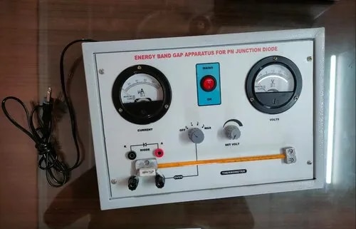
Energy Band Gap of PN Junction Diode
Description
The “Energy Band Gap of PN Junction Diode” refers to the minimum energy required to move an electron from the valence band to the conduction band in a semiconductor material used for making diodes, typically measured using a reverse bias experiment on the diode.
Principle and Theory
The energy band gap (E
g
g
) is the energy difference between the top of the valence band and the bottom of the conduction band in a semiconductor. For a PN junction diode, this gap correlates with the minimum energy an electron needs to enable conduction.
When a diode is reverse biased, the minority carrier concentration determines the reverse saturation current, which strongly depends on temperature due to its relationship with the band gap energy.
Experimental Description
Apparatus:
Includes a PN junction diode (silicon or germanium), a microammeter, a voltmeter, a thermometer, and an electric oven to vary junction temperature.
Procedure:
The diode is reverse biased and placed in a temperature-controlled oven. As the temperature is changed, the reverse saturation current
I
s
I
s
is measured at different temperatures.
Data Analysis:
A graph is plotted of
log
10
(
I
s
)
log
10
(I
s
) vs.
10
3
/
T
10
3
/T (where
T
T is the temperature in Kelvin). The straight line's slope is used to calculate the energy band gap using:
E
g
=
slope
5.036
E
g
=
5.036
slope
(value in electron volts for silicon is usually around 1.1 eV and for germanium about 0.7 eV).
Applications
Accurate determination of the energy band gap informs about the electrical and optical properties of semiconductor devices, influencing their performance in electronics and optoelectronics.
This experiment provides insight into semiconductor theory, band structure, and the physical limits of conduction in diode materials.
Specifications
| Model No. | N-EL037 |
|---|


